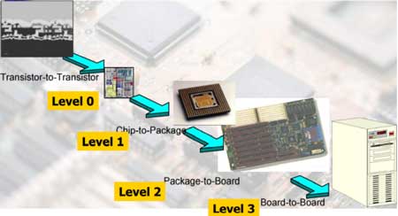
Who Can Solve the “Hidden Problems” of Chip Packaging and Testing in the Wave of AI Chips?
Packaging and testing are the final steps in the chip manufacturing process. Packaging is responsible for protecting, securing, and electrically connecting the bare chips diced from the wafer, enabling them to communicate with external circuits. Testing, on the other hand, uses a series of electrical performance tests to screen out qualified chips, ensuring the reliability of the final product. Within the testing phase, there is a seemingly insignificant yet crucial component—the chip packaging test spring. It is responsible for accurately positioning the chip and transmitting test signals, directly determining the accuracy of test data and the final chip yield; it can be considered the “invisible guardian” of the packaging and testing process.
The current AI wave is sweeping the globe, and chip integration continues to improve. Advanced packaging has become key to breakthroughs in AI chip performance, acting like a foundation supporting the upper-level computing power. According to multiple market research institutions, the global advanced packaging market is growing rapidly and is expected to reach tens of billions of dollars in the next few years. As a crucial link in the global semiconductor industry chain, China’s share in advanced packaging is also continuously increasing. However, behind this prosperity lies the anxiety of countless packaging and testing companies working late into the night.
Many packaging and testing companies invest heavily in upgrading advanced packaging equipment to secure AI chip orders, with investments exceeding one million yuan per wafer. While wafer manufacturing yields can reach industry-leading levels of over 99%, the yield plummets to below 80% once the packaging and testing phase begins. Even more problematic is the insufficient precision of the contact springs; a tiny deviation of 0.5μm can cause the entire chip to fail. Under high-temperature testing conditions, the contact springs are prone to stress relaxation and performance degradation, rendering the initial investment worthless and leading to customer returns and claims. With order backlogs extending two years into the future, these companies are hesitant to accept new orders due to contract spring issues, watching business opportunities slip away.
While chip packaging and testing springs may seem simple in structure, they are the core carriers for chip aging and packaging testing. Their positioning accuracy and signal transmission stability directly determine the test accuracy and final yield.
Currently, most springs in the industry have obvious shortcomings: ultra-thin models are prone to deformation, and their performance degrades quickly under high temperature conditions; small-batch customization makes it difficult to balance accuracy and delivery time, and some finished products even require secondary testing, which seriously slows down the production progress and increases labor costs.
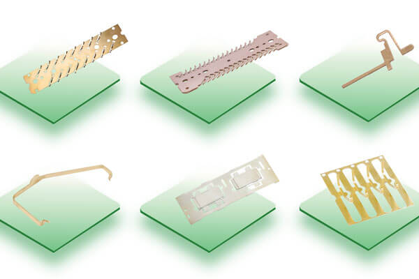
Dongguan Heju Precision Electronics Technology Co., Ltd., with over a decade of experience in the field of precision springs, has long recognized the core anxieties of packaging and testing companies. As a professional manufacturer of chip packaging and testing clips, Heju Precision’s offer clips with a complete range of specifications, long service life, and precise matching of the high requirements of advanced packaging in the AI era. They perfectly avoid the pain points commonly found in the industry, such as insufficient precision, unstable performance, and delayed delivery. With its solid strength, Heju Precision provides packaging and testing companies with the confidence to break through bottlenecks and seize the AI opportunity.