Something About Semiconductor Chip Aging Test
No matter where we go, we are always surrounded by technology. Our smartphone has become an indispensable tool in our daily life. These different technologies need an indispensable component -the semiconductor, regarded as the brain of modern electronic products. Similar to any electronic device, we need to ensure the reliability of this key component so that our equipment can run normally.
So how can manufacturers improve the likelihood of delivering the best possible product to the end user? This must be done through rigorous semiconductor testing.
One of the most common and important semiconductor chip testing protocols is aging testing, is used to detect early failures of components and reduce the likelihood of defects and failures during use.
The Purpose of the Semiconductor Aging Test
Consumers pay a high price for their electronic devices, and the last thing they want is for a product to malfunction after purchase. The semiconductor aging test replicates the on-site stress environment and simulates various situations, thereby reducing the failure rate.
Only aging testing performed on large samples allows manufacturers to better understand how semiconductors will perform in real-world applications. Through this process of elimination, manufacturers can minimize the number of defective semiconductors they ship to customers. This approach increases the likelihood that an electronic device will meet the level of reliability consumers expect. Therefore, aging testing is essential to ensure the quality control of the production line.
How is the Aging Test Carried Out?
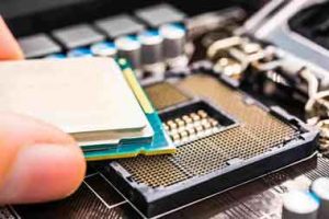
During the test phase, semiconductor components are fixed on burn-in boards and then placed in burn-in systems such as environmental chambers. In this laboratory, latent defects in semiconductors are detected through a medium. When the device is subjected to voltage stress and heating while operating, special springs are activated. In order to make the chip’s latent defects stand out in the process.
Depending on the test scenario, these operating conditions may include exposing semiconductor components to extreme temperatures, varying voltages/currents, high operating frequencies, or any other conditions classified as upper limits by subjecting components to carefully calibrated Severe conditions allow technicians to identify underperforming parts without compromising the life of good parts.
The purpose of these aging tests is for the manufacturer to collect enough data to form a bathtub curve (example below) and reduce semiconductor failure rates.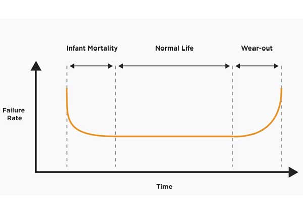
During the initial testing phase — “classified as infant death” — many semiconductors experience early component failure. These failures are often the result of manufacturing defects, which are becoming more common due to aggressive technology scaling and increased circuit complexity.
The root cause of these defects can be identified as conductor failure, electromigration, dielectric failure, metallization failure, etc. These defects cannot be found by traditional quality assurance testing and may appear randomly during the device’s life cycle. Therefore, semiconductor components must be tested intensively before such problems manifest as failures.
However, although the failure rate decreased over time, the results were not ideal during infant mortality because a large number of failures still occurred in a short period of time. Delivering semiconductors at this stage will result in customer dissatisfaction and high warranty costs.
Conclusion of Aging Tests
With the feedback gathered from burn-in testing, the manufacturing process can be improved to reduce failure rates. While components may still fail over time, the intent is to ensure that these failures generally occur during the normal life phase of the product’s useful life.
Theoretically, failures can still occur randomly during the normal lifetime of a semiconductor. However, when measured over an extended period, these problems typically manifest at a relatively constant rate, resulting in high warranty costs for the manufacturer. So, they would want the bottom of the bathtub curve (failure rate) to be as low as possible. And any wear-and-tear failures that occur during the expected lifetime of the semiconductor must also be addressed before the product is ready to ship to the customer.
Another key detail to note is that burn-in tests are also performed on deliverables. Therefore, these evaluations are less intensive than accelerated life testing. These semiconductor components also spend less time in burn-in testing than in ALT testing (Accelerated Life Testing). After all, manufacturers don’t want to compromise the useful life of their products.
Choose a Reliable Stamping Supplier for Your Semiconductor Chip Project
Dongguan Heju Precision Electronic Technology Co., Ltd. is a professional stamping manufacturer of chip packaging and testing clips. It can provide corresponding solutions according to the different needs of customers. The chip packaging and testing shrapnel has many specifications and long life, which meets your testing requirements. In terms of absolute precision and repeatability of the product, rapid prototyping of any complex hemming structure can be realized!