Lead Frames on Chip Package in Semiconductor Industry
Definition of Lead Frame
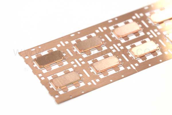
A lead frame is a metal structure inside a chip package that brings signals from the die to the outside, utilized in DIP, QFP, and other packages where links to the chip are made on its edges.
The lead frame’ structure consists of a central die pad, where the die is placed, bordered by leads and metal conductors diverting from the die to the outside world. Each lead closest to the die was completed in a bond pad. Little bond cords attach the die to each bond pad. Mechanical links fix all these components into a rigid framework, instantly making the whole lead frame easy to manage.
Production of Lead Frames
Lead frames are made by eliminating material from a flat plate of copper, copper alloy, or iron-nickel. There are two processes used for this production: etching and stamping. The mechanical bending process can be used after both techniques.
As soon as mechanical bending is settled, The die is glued or soldered to the die pad inside the lead frame, and after that, bond wires are attached between the die and the bond pads to connect the die to the leads. And then, Encapsulation is performed when a plastic case is formed around the lead frame and dies so that only the leads are left exposed. As soon as Encapsulation is complete, the leads are cut off outside the plastic body. And any revealed supporting structures are removed. The outside leads may be bent to any needed form that fits the details application to finalize the item.
Etching Or Stamping?
-
Chemical Etching
As a whole, Etching is used for high-density leads as it can give much closer tolerances and finer detail. For instance, high-density QFN (close to the die’s dimension) kind assemblies are generally etched. Etched lead frames are produced in flat sheets. Usually constructed out of either copper or iron-nickel alloys (such as alloy 42) that show a very low expansion rate at room temperature level. These low thermal expansion alloys have discovered usage in modern applications. That require joining metal to glass or porcelains and in areas that need the same thermal expansion rates for products to be entered to prevent associated issues within the joint location.
-
Stamping
Stamping is the favored automated process for low lead density and more extensive package assemblies. People generally use it in high-volume manufacturing runs. The sheet metal material is punctured along both sides to develop indexing holes that position the sheet during further processing. The location holes are utilized to progress the sheet metal strip with the stamping machine. Die-and-punch collections particular to the lead frame geometry are also needed. The procedure is typically completed by a series of stamping operations that progressively approach the final lead frame geometry, the variety of actions being based on the intricacy of the geometry of the lead frame.
Use of Lead Frames
Lead frames are made used to manufacture a quad flat no-leads package (QFN), a quad flat bundle (QFP), or a twin in-line bundle (DIP).
In Conclusion
Over time, as our criteria progress and our needs expand, there has been a need for far more accuracy in the manufacturing and packaging process of integrated circuits and semiconductors. There are many lead frames, each characteristic varying based on the individual’s requirements. Usually, modification is carried out to satisfy required specs, attributes, thermal properties, and electric residential properties. Please email us for more details concerning your precision stamping project for lead frames.