Comprehensive Analysis of COC Fishbone Fixtures in Burn-in System
August 5, 2026

Comprehensive Analysis of COC Fishbone Fixtures in Burn-in System

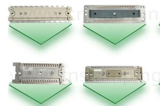
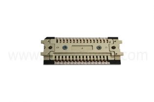
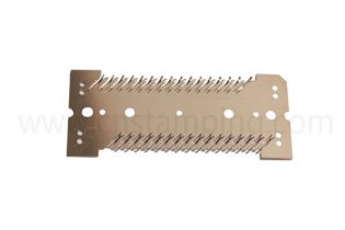
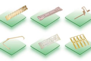
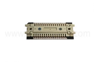
The COC fishbone fixtures in Burn-in System, with its fishbone array-like design, integrates positioning slots, beryllium copper elastic contact springs, and thermally conductive trenches. It is a key high-value consumable in the production and testing of optical modules, primarily used for burn-in tests of optical chips. Its core function is to provide precise positioning, stable

COC Burn‑In Fishbone Fixtures: How They Supercharge Chip Reliability Screening
July 28, 2026

COC Burn‑In Fishbone Fixtures: How They Supercharge Chip Reliability Screening

Let me draw you a picture. You’ve just finished a run of high-power laser diodes. You send them to burn-inin testing — 24 hours at 85°C with a constant current — and when they come out, half of them have degraded. Not because the chips are bad, but because your socket killed them. Poor contact.

Selection of 5 key parameters for Chip Burn in Test Fixtures
May 26, 2026

Selection of 5 key parameters for Chip Burn in Test Fixtures

Engineers performing chip aging tests know one thing: No matter how well designed the burn-in board is or how precise the temperature control is, a malfunctioning aging test fixture ruins the entire experiment. Intermittent contact problems, probe shrinkage at high temperatures, and chip cracking from cap deformation are common in mass production aging. Most issues

Chip Aging Test Fixture Selection Guide: From Principles to Key Considerations
May 19, 2026

Chip Aging Test Fixture Selection Guide: From Principles to Key Considerations

In the semiconductor industry, it’s said: “A chip untested for aging can’t be trusted for vehicle use.” This refers to chip burn-in testing. The tool used is the chip burn-in test fixture, commonly called a burn-in socket. Many associate it with simply “a socket holding a chip at high temperature,” but engineers experienced in mass

Applications of Chip Packaging and Testing in the Semiconductor Industry
April 14, 2026

Applications of Chip Packaging and Testing in the Semiconductor Industry

Chip Packaging and Testing: A Key Link in the Semiconductor Industry Within the expansive semiconductor industry, chip packaging and testing are critical technical processes. Chip packaging and testing, also referred to as assembly and test, entails enclosing chips produced by wafer fabrication and subjecting them to rigorous performance evaluation, turning them into finished chips ready

Who Can Solve the “Hidden Problems” of Chip Packaging and Testing in the Wave of AI Chips?
April 7, 2026

Who Can Solve the “Hidden Problems” of Chip Packaging and Testing in the Wave of AI Chips?

Packaging and testing are the final steps in the chip manufacturing process. Packaging is responsible for protecting, securing, and electrically connecting the bare chips diced from the wafer, enabling them to communicate with external circuits. Testing, on the other hand, uses a series of electrical performance tests to screen out qualified chips, ensuring the reliability