Applications of Chip Packaging and Testing in the Semiconductor Industry
Chip Packaging and Testing: A Key Link in the Semiconductor Industry
Within the expansive semiconductor industry, chip packaging and testing are critical technical processes. Chip packaging and testing, also referred to as assembly and test, entails enclosing chips produced by wafer fabrication and subjecting them to rigorous performance evaluation, turning them into finished chips ready for use in electronic devices.
Chip packaging primarily shields the chip from environmental hazards while enabling electrical connectivity and structural support. Common methods include dual in-line packages (DIP), ball grid array (BGA), and chip-scale packages (CSP). Each method has distinct features and ideal use cases. DIP offers lower cost and suits simple, low-performance circuits; BGA provides higher pin density and superior heat dissipation for high-performance chips.
Chip testing ensures packaged chips meet design and quality standards. Wafer testing checks basic functions; final product testing provides a comprehensive assessment after packaging. The following table compares the characteristics of different encapsulation methods:
| Packaged Type | Advantages | Disadvantages |
|---|---|---|
| DIP | Low cost and simple process | Limited pins number and Large volume |
| BGA | High pin density and good heat dissipation | High cost is and complex process |
| CSP | Small size and high performance | high requirements for packaging technology |
Applications of Chip Packaging and Testing in the Semiconductor
Chip packaging and testing technology have wide applications in the semiconductor industry. First, it improves the reliability and stability of chips, enabling them to operate normally in complex environments. Second, packaging technology allows for chip miniaturization and integration, meeting the demands for thinner, lighter, and higher-performance electronic devices. Third, the packaging and testing process allows for chip screening and classification, improving yield and reducing production costs.
With the ongoing advancement of semiconductor technology, chip packaging and testing methods are rapidly evolving. For instance, advanced 3D packaging enhances chip integration and performance, while fan-out packaging offers innovative solutions for high-performance chip assembly.
In conclusion, chip packaging and testing are essential to the semiconductor industry. Advancing these technologies creates new opportunities and challenges, pushing the industry toward higher performance, smaller size, and lower cost.
Heju-Reliable Chip Packaging and Testing Contact Spring Manufacturer
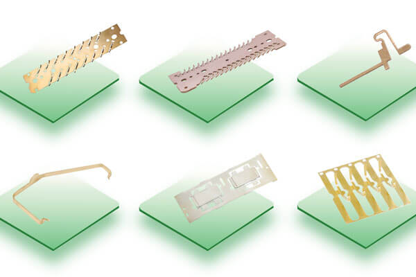
Dongguan Heju Precision Electronics Technology Co., Ltd., with over a decade of experience in the field of precision springs, has long recognized the core anxieties of packaging and testing companies. As a professional manufacturer of chip aging packaging and testing contact springs, Heju Precision’s offer contact springs with a complete range of specifications, long service life, and precise matching of the high requirements of advanced packaging in the AI era. They perfectly avoid the pain points commonly found in the industry, such as insufficient precision, unstable performance, and delayed delivery. With its solid strength, Heju Precision provides packaging and testing companies with the confidence to break through bottlenecks and seize the AI opportunity.