
Burn-In Test Contact Arrays: When a Micro-Burr Melts Your Yield
Many times, when people say “semiconductor burn-in sockets,” they will think of pogo pins — single spring-loaded plunger assemblies placed within a plastic block. But if you look at the image above, you’ll see a completely different beast.
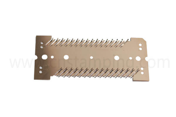
This is either a stamped contact interposer or a cantilever contact spring sheet. This is one long continuous piece of metal, typically made out of high-performance beryllium copper (BeCu) and has many dozens of ultra-fine, comb-like cantilever beams protruding from the center.
As each individual “feather” is forced against the solder ball or gold bump of the IC during its insertion into the test socket, it operates as a separate electrical connection, rubbing across the surface.
The item appears to be of good quality; however, it is a very difficult process to stamp, plate, and inspect. If the tooling is slightly off, the item can cause significant damage to the HTOL data.
The actual process that takes place on the test floor using these types of arrays, as well as the items you should verify prior to purchasing such arrays, are detailed below.
The Coplanarity Nightmare: One High Finger Cracks the Chip
Since each contact finger is formed from one piece of material, they have to maintain the same level of coplanarity—meaning they must be as flat as possible relative to each other.
The following will occur if you bend one of the cantilever beams even slightly higher than required:
That one finger takes all the mechanical load.
It acts like a tiny spike, creating a stress point on the chip’s solder ball.
The chip can crack under the compression force.
Or, conversely, a finger sitting too far down will never make contact, resulting in a periodic open circuit.
At this point, the stamping die and heat treatment must have zero defects. In our production of high-density burn-in contacts at Heju, there is no wiggle room for error on the flatness tolerance of each contact array. If the sheet gets warped during stamping, you can’t correct it later. Therefore, the stamping die must be designed to produce a perfectly flat product with every stroke.
The Burr Problem: Scratching the Gold Bumps
Look very carefully at the very tip of each one of those cantilever fingers. In order to effectively break through the thin layer of oxide that covers the pad on your chip with a “wipe” action, these tips must be extremely sharp. But “sharp” is very different from “burred.”
The micro-burr at the top of each finger in a stamped contact spring can act as a miniature razor blade. When an operator loads the chip into the array and the fingers pass over the surface, the burr can remove the gold bumps from the die or flatten the solder balls.
Furthermore, the tiny metal particles (debris) left in the socket after removing the burr will remain there. When you close your computer again, the loose metal will create an electrical short circuit between two side-by-side pins.
The die for the stamp needs to be designed so it can cut through the metal cleanly. At Heju, we closely control the die clearance to provide a sharp enough tip to clean off the material being worked on; however, there are no burrs left behind on the tip, which might cause harm to the item being tested.
Stress Relaxation at 150°C: The Spring That Forgets to Bounce
A burn-in test is a long-term environmental exposure to high temperatures and voltages. It’s not a short-term, in-and-out type of functional test. The test socket will be in a temperature-controlled environment (thermal chamber) for 1000 hours, at temperatures ranging from room temperature up to 150°C. During this time, the chip will receive continuous electrical power (voltage).
Because of its resistance to stress relaxation, beryllium copper (BeCu) is considered the “gold standard” for cantilever contact spring applications. However, all types of BeCu are not produced identically.
When the heat treatment (aging) that occurs after the stamping is off by just a few degrees, or if the stamping process creates residual stress in the bend radius of each of the finger-like springs, then they will slowly lose their tension as they go through the oven. As the normal force decreases, the contact resistance increases, and the temperature at the interface rises; therefore, your good chips will ultimately fail the testing procedures.
When you order your arrays, you should inquire with the manufacturer regarding the condition of the material after being stamped, and the type of thermal processing that has taken place on the product after stamping. If the manufacturer simply purchases a sheet of BeCu and bends it without undergoing a controlled age-hardening process, then your HTOL testing results are going to be very poor.
Why Custom Stamping Beats Etching
Chemical etching is preferred by some engineers to produce the contact sheets because it does not result in burrs from mechanical cutting. However, there are problems associated with chemical etching, including the fact that the process results in the metal becoming brittle. Additionally, the process can cause the edges of the sheet to become tapered, negatively affecting the mechanical function of the spring.
A good progressive die stamping process produces a better part. It produces clean edges because of mechanical shearing, and the metal gets “grain” from being bent. This grain can then be made better for spring forces.
However, to make the ultra-fine, high-density fingers shown in the photo, you will need a great deal of tooling capability. You need to use a carrier strip that will keep your parts absolutely still during the entire stamping and plating processes. If the carrier strip moves at all, then the finger width will vary.
We have chosen to create all of our progressive dies on-site because we can regulate each step of the die-making process (i.e., die clearance, heat treatment and selective plating), which allows us to ensure that the mechanical force applied by each finger will be consistent.
What to Ask Before You Buy a Burn-In Test Contact
Don’t simply submit a request for quote (RFQ) for a “test spring” when developing a burn-in socket or a test interposer for high-pin count devices. Ask your precision BeCu stamping partner:
- What is the flatness (coplanarity) spec across the entire array?
- How do you control burrs on the contact tips?
- What is the stress relaxation rate at your operating temperature?
- How do you ensure the plating (typically hard gold) covers the entire length of the finger, but does not cause the fingers to bridge together?
HejuStamping-Precision Contact Springs Supplier in Burn-In Test System
At HejuStamping, we focus on precision stamping of high-performance components. We understand that your contact array has to be mechanically perfect, as well as electrically stable. Whether you have a failing socket design or need a custom contact sheet stamped, send us the drawing. Our engineers can provide you with a straightforward answer as to whether or not it is possible to create tooling, and how well we can maintain tolerances.
Reach out to us at www.cnstamping.com. We won’t give you a sales pitch, but we will provide you with honest, technical advice.